Event input using the evaluation board
Applicable receivers: BD940 | BD940-INS | BD970 | BD982 | BD990 | BD992 | BD992-INS
This topic describes how to condition and analyze event input signals when using the OEM GNSS I/O development boards. This knowledge also applies to the customers’ implementation of event inputs on their carrier board for the BD9xx.
Useful links:
-
For information about the web interface settings, see the topic, Receiver Configuration – General.
-
Application note: Event (0) 1PPS Input Example.
-
For Event 1 and Event 2 information, see below.
Event
|
Item |
Description |
|---|---|
|
Event 1 |
On the BD940 receiver module, pin 37 is dedicated as an Event_In pin. On the BD940-INS receiver module, pin 15 is dedicated as an Event_In pin. On the BD970 receiver module, pin 8 is dedicated as an Event_In pin. On the BD982 receiver module, pin 8 is dedicated as an Event_In pin. On the BD990 receiver module, pin 8 is dedicated as an Event_In pin. On the BD992 and BD992-INS receiver modules, pin 8 is dedicated as an Event_In pin. This is a TTL-only input; it is not buffered or protected for any inputs outside of 0 V to 3.3 V. It does have ESD protection. If the system requires event to handle a voltage outside this range, the system integrator must condition the signal before connecting to the unit. |
|
Event 2 |
On the BD940 receiver module, pin 39 is dedicated as an Event_In pin. On the BD940-INS receiver module, pin 7 is dedicated as an Event_In pin. On the BD970 receiver module, pin 7 is Event 2; however, it is multiplexed with COM3_RX and CAN_RX. The default setting is to have this line set to COM3_RX. The Event 2 must be enabled to use Event2. On the BD982 receiver module, pin 7 is Event 2; however, it is multiplexed with COM3_RX and CAN_RX. The default setting is to have this line set to COM3_RX. The Event 2 must be enabled to use Event2. On the BD990 receiver module, pin 7 is Event 2; however, it is multiplexed with COM3_RX and CAN_RX. The default setting is to have this line set to COM3_RX. The Event 2 must be enabled to use Event2. On the BD992 and BD992-INS receiver modules, pin 7 is Event 2; however, it is multiplexed with COM3_RX and CAN_RX. The default setting is to have this line set to COM3_RX. The Event 2 must be enabled to use Event2. This is a TTL-only input; it is not buffered or protected for any inputs outside of 0 V to 3.3 V. It does have ESD protection. If the system requires event to handle a voltage outside this range, the system integrator must condition the signal before connecting to the unit. |
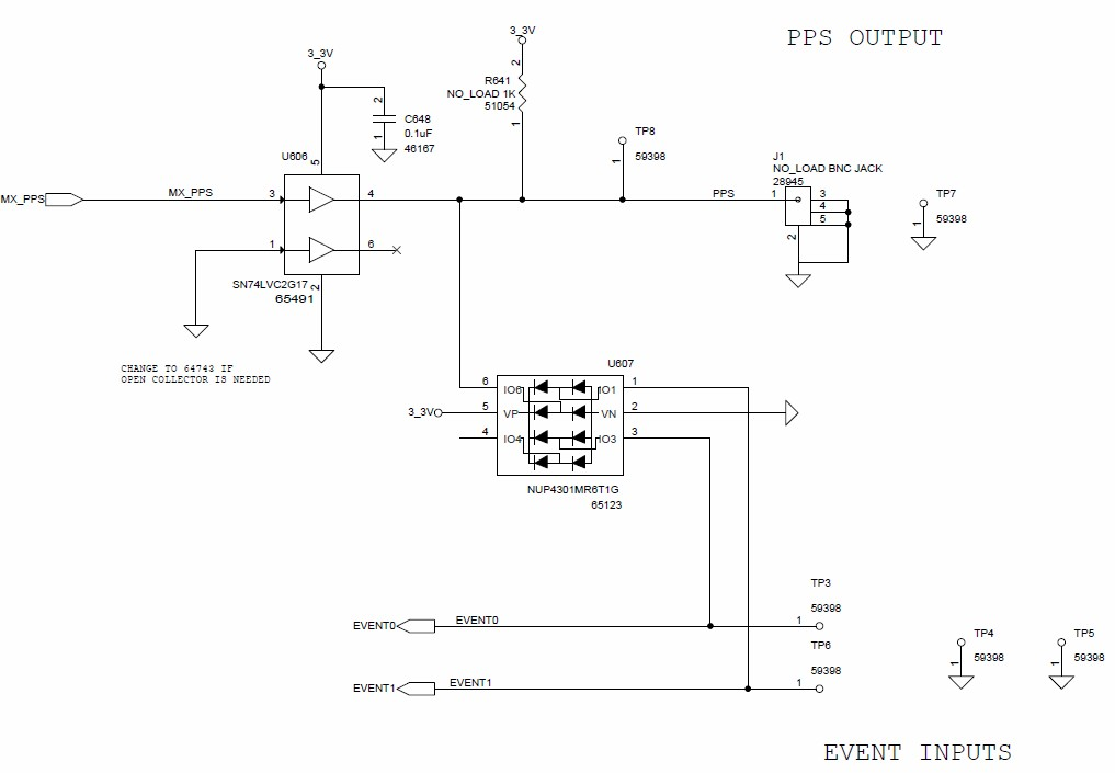
Event schematics of the BD9xx evaluation PCB
Trimble recommends adding a Schmitt trigger and ESD protection to the Event_In pin. This prevents any "ringing" on the input from causing multiple and incorrect events to be recognized.
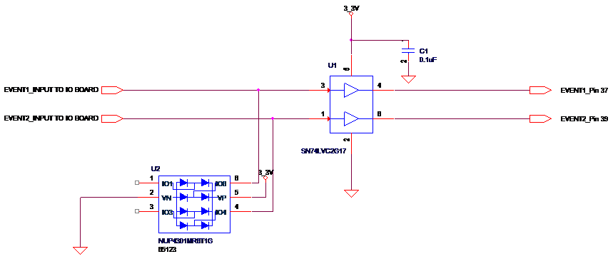
PPS output and event inputs BD940
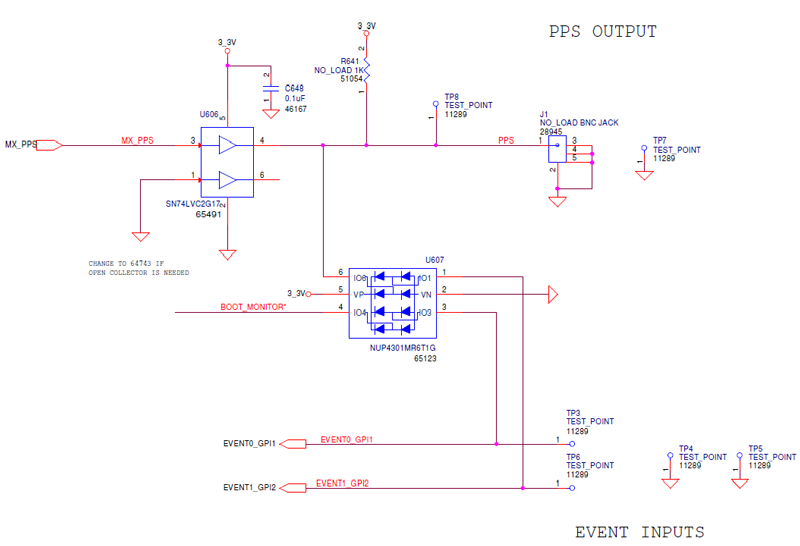
PPS output and event inputs BD40-INS
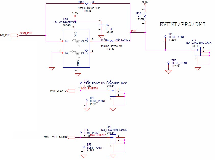
PPS output and event inputs BD970 and BD982
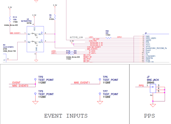
PPS output and event inputs BD990, BD992, and BD992-INS